
Home Page for Ajawamnet
& Wayne Mitzen
Click here for misc. links
|
Home Page for Ajawamnet & Wayne Mitzen Click here for misc. links |
| Over 35
years of design experience - I have a full lab here in A traditional resume and portfolio can be downloaded here in PDF format and is also located at the end of this webpage . I've designed over 3,000 products since the late 1970's. These include RF, mixed mode analog and high-speed digital. Familiar with various protocols including PCI/PCIe, HDMI, DP, USB 2/3, CAN Bus, RS232/422/485, SPI, SSI/Stegmann for encoders/resolvers, DDR3-5. I have developed designs spanning PCB stack ups over 30 layers. I've designed rigid-flex that included differential signaling. I hold three patents including one in 1995 for the one of the first wireless IoT systems (see below). | |
 |
My experience
includes designs for various consumer markets as well as many
industrial and government/military applications. In most cases my wife
and I can quickly deliver assembled prototypes/small
production builds as well. This includes fine pitch SMT, which can
easily be ported into full electronic documentation for use with
automated assembly processes for ramping up into full-scale production.
I will work with any contract manufacturer the client selects or can
offer suggestions based on the scope of the project. In addition to the SMT rework/assembly equipment, I maintain a full CNC shop for rapid turnaround of the mechanical aspects of those projects. I can perform the electrical and mechanical design, then actually deliver complete working proto/EAP products in the target form-factor.
|
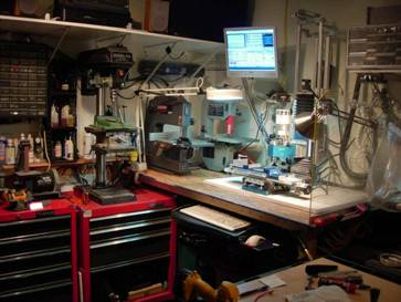
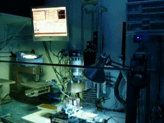
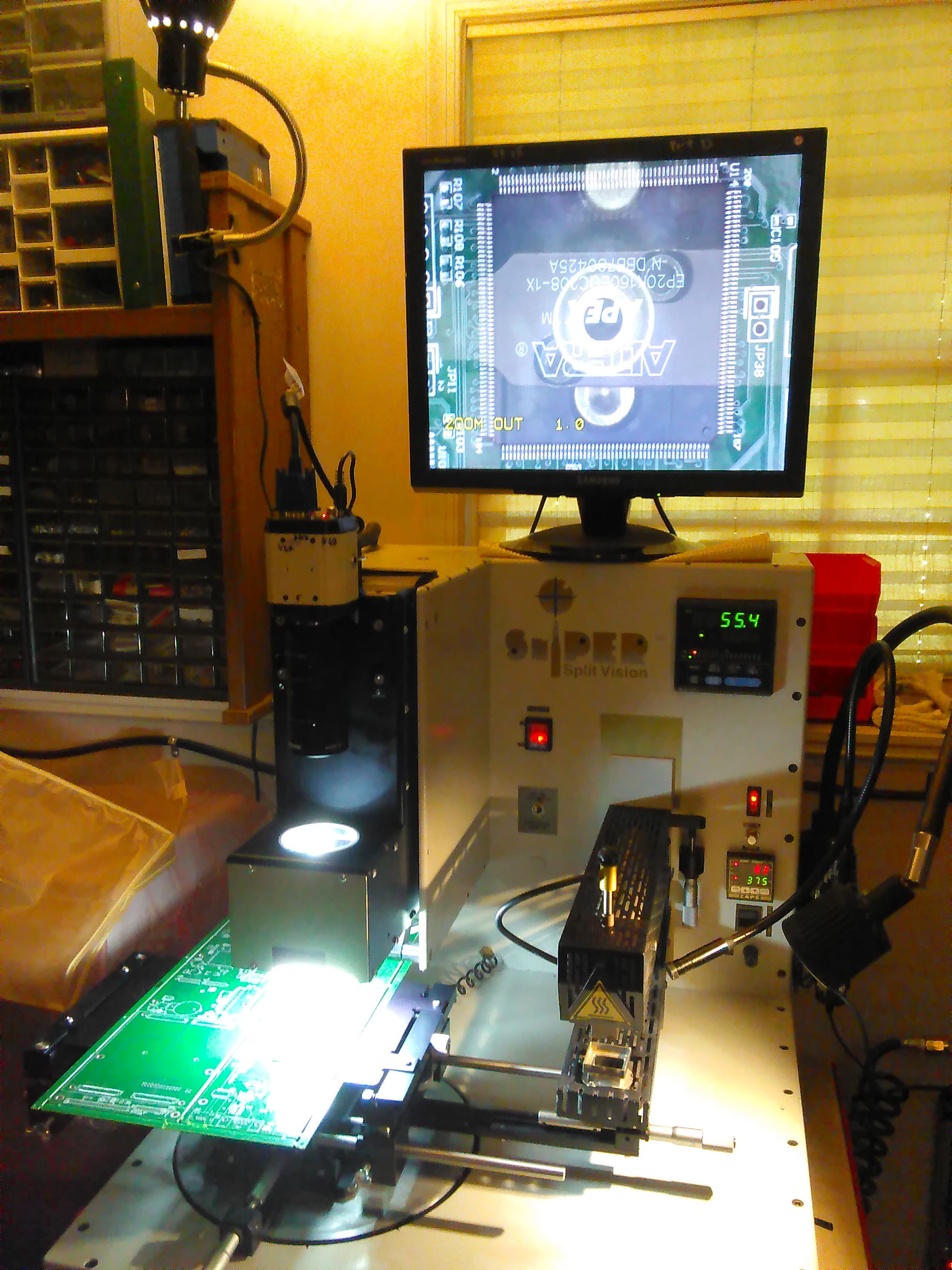 Split vision BGA Rework station |
 Link to vid of placement |
| I did some of the first
designs for the original IBM XT, running DOS 1.1; it was for
the video CGA adapter. At the time, there were no clones, no reference
designs on developer.intel.com (the internet wasn't really even
accessible to common-folk), and the main method to layout multi-layer
PC boards was to use Bishop Graphics 4:1 tape up (red and blue decals
on velum). My device allowed the use of these early PC’s with the
various projection and video production systems that were available in
1984. These were sold to various Westinghouse divisions, as well as
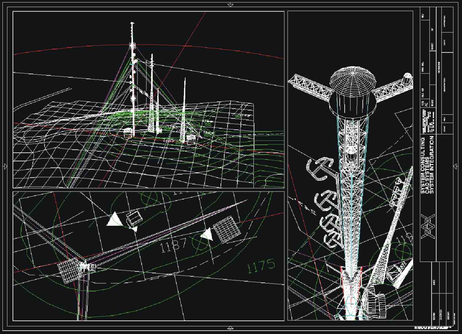
many universities (one of the first devices installed at CMU’s Since 1990, I was one of the early proponents of using the emerging EDA tools, one of which was the original ORCAD family of DOS based products, as well as doing some of the first 3D modeling with AutoCAD version 10. After the fiasco of the ORCAD port to Windows, I switched to Protel (version 3) and have since used Altium’s line of products; though I am still proficient in ORCAD as well as a myriad of other EDA/CAD tools. All of the 500+ products I've designed since then typically consist of digital, RF, and analog (full SPICE modeling) topologies used in various applications with support for programmable logic, various uC an uP architectures including low-power embedded designs. As to mechanical design (both MEP and packaging), I was one of Solidworks first customers. I had been doing Autocad 3D surfaced modeling in the early 1990's Here's a link to a cool ACAD file from the early 1990's : http://www.ajawamnet.com/ajawam4/trans.dwg It was done in 1992 in AutoCAD version 10, NO MOUSE or DIGITIZER, on a 80386SX-25 with 4Meg of RAM on a 14" amber screen CRT. All command line call outs and cursor keys. Those convoluted arms are ERI 40kW FM circular polarized antenna bays. They stack 4 at a 1/4 wavelength for antenna gain (ERP). The green lines are USGS topo, the grid is a 5' topo from the county (Hazelwood in Pgh). The entire drawing is at the correct height above the ACAD world coordinate, so you can get the AMSL. It opens in PSPACE; just do a MODEL command or hit the model tab, then do a Plan - Current UCS. The dot at the UCS is a tower farm, the line is the line of sight for a terrestrial microwave path. If you do a Time command in AutoCAD: Times for this drawing: Created: Saturday, December 12, 1992 at 3:41:12:630 PM JPG of the PSPACE plot: http://www.ajawamnet.com/ajawamnet/page4/towers.jpg I saw the advantage of parametric solids as soon as Solidworks 1995 was released. Took a bit to get used to ("where's the dang UCS?") but was worth it. I still have my Solidworks 1996 install CD (when it still fit on a CD). I was doing SLA's 3D printing back in 1997 - the example on the right was initially printed that way for form-fit checking. |
Over 3,000 designs completed with Altium since 1995  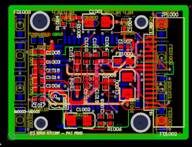 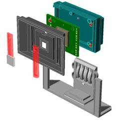 Injection molded
part
Injection molded
part |
| Link to Edwg of above image |
|
I've pioneered development in many areas, including some of the first ISM-based RF devices and I was one of the first to embrace the use of CMOS imagers in commercial applications. I hold a patent for a company I co-founded (Inventor, USPAT 6,208,266 for Remote data acquisition and processing system) that used some of the first CMOS imagers available from Motorola, FUGA, Omnivision, VLSI Vision. https://www.google.com/patents/US6208266 The patent also discusses using various methods to connect these remote telemetry devices to the Internet. Wirelessly in fact... Yea, I know. They now call it "The Internet of Things" or maybe part of "The Internet of Everything" Oh well... isn't it great when they now label something you did years ago in 1994? See my marketturd link: http://www.ajawamnet.com/ajawamnet/mama_i_wanna_be_a_maker.html For some reason the Google PDF download is not searchable. So here's a PDF generated from the Google site that is: Search it for the word Internet.... Interesting to see GE citing it in their patent 6,411,678 (see the References section of the link to google patent listing). And it seems like a lot of patents reference it... that's usually a sign that it was significant in some future thing that makes money. Sigh....If you read the very end of the aforementioned " Mama I wanna be a Maker " rant on my Marketturd site - I guess I'm more like the Woodcarver in Tao -I try to do things for the right reasons. Not so much for shiny rocks and paper with president's pics on it. It was a great ride with some great people in it. Also note - the enclosure for the prototype of the first unit that was demo'd at a funding event at the Harvard Business Club in 1995 was 3D printed - yep SLA'd. It's starting to melt now. 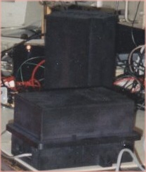 I'm also on other
patents for technology such as one for a secure device used
by governments and industry to allow uni-directional transfer of data
between networks (also known as cross domain systems) (Inventor,
USPAT 8,250,235) as well as one for wireless
intrusion detection (Inventor,
USPAT 7,778,606) with that device making the cover of
Government Computer News (I can provide a PDF re-print of the GCN
article if necessary). I've also developed many products for industrial automation, telecommunications, core network, and network-based security (IDS, firewall, crypto) appliances. All in all I've designed well over 500 products in the past eight years with number probably at 1000 for the entire 18 years of experience in product design. Not in a cursory capacity, but usually in "concept to production" capacities. I have numerous references, a lot of them in the DC area. I recently won accolades as being one of the best full turnkey PCB design services in the "Much thanks to "... but because we have had so many instances of other people who have done software for us that didn't quite work. It has been a real blessing to [company name] to have worked with you, and Wayne (duuude) on the hardware side, on our projects over the last year or two. You guys give us a lot of confidence in the things that we are trying to do." |
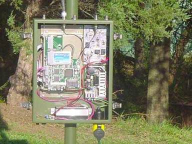
| An example of a military
application In typical real-world scenarios, development of a product, regardless of the market, usually requires a team that can deliver products in a very short time frame and still hit all the functional aspects of the product specification. Occasionally, this is accelerated when new clients approach me that are already well behind schedule and way over budget. Add to that the bureaucracy involved after being selected as a developer; getting the proper contract vehicles in place with primes, various departments, etc., and it can severely impact the time left to actually develop the product. This was the case with a recent project; it consisted of a small multichannel wireless ADC device as well as a wireless handheld device in a submersible container - you may have seen similar enclosures on web sites for "Area 51 sensors" recently (you can google that exact phrase - usually in the first link that comes up ). Even with the constraints of both time and resources, Sanjay and I were able to specify, model, and create initial prototypes in less than three weeks. As we got further into it, we along with the team from the military and the contractor, learned that the spec which was originally written in 1988 was not clear on a lot of the technical aspects of the target systems. This led to further refinements, and in the case of the wireless ADC device, a significant change to the circuit topology. Even with these issues we were able to get 10 new sets of the modified design completed and ready for FAT (First Article Testing) as per the military requirements in less than a month. This included a change to the mechanical system for the handheld, as well as a vendor suddenly EOL'ing (end-of-life'ing) a "new" OLED display without warning (Digikey still showed the product as "new" when the product manager at the vendor mentioned them killing the product line). This also required setting up and machining various mechanical aspects of including enclosure modifications, fixtures for assembly and actual part fabrication to satisfy the "adjusted" requirements. Not to mention my poor wife having to hand place over 4,000 SMT parts (0603 passives), sometimes in less than three days. The units passed FQT, withstanding MIL STD 883 tests that even the GFE simulators used to test our devices would shutdown or reset during the tests. For example, when testing our DCA device, I injected ~8KV to our PCB ground; our device didn't even hiccup but the simulator crashed with the attached Windows application laptop rebooting back to a BIOS screen as well. After a few more tests, we were able to assemble another set of fifteen units that eventually passed the second tests known as FQT. |
  Solid Models of both the DCA and Handheld unit 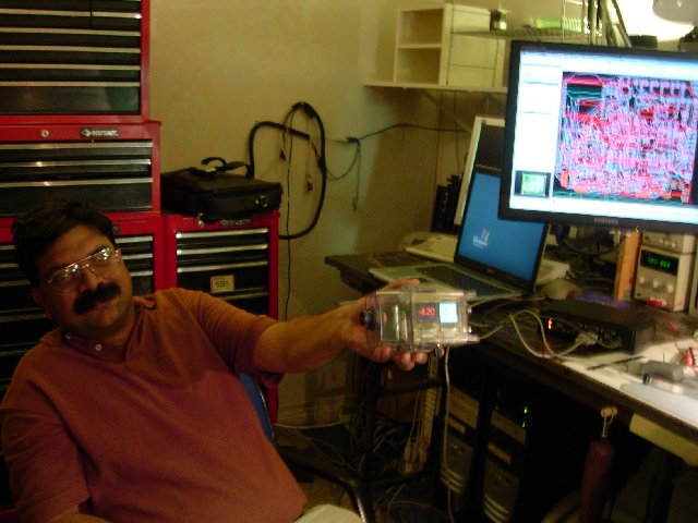 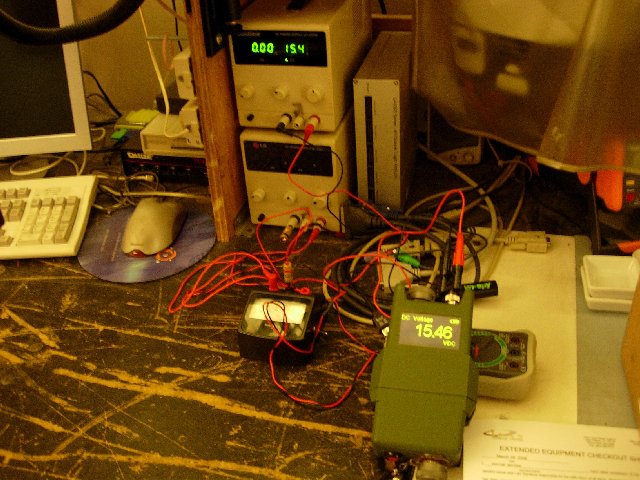 Pictures of Sanjay with the initial prototype and a picture of the completed FQT unit 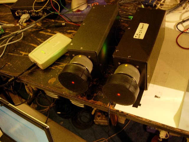 Wireless DCA device under test on GFE military simulators |
Hardware and PCB Design and Layout |
|
 |
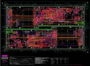
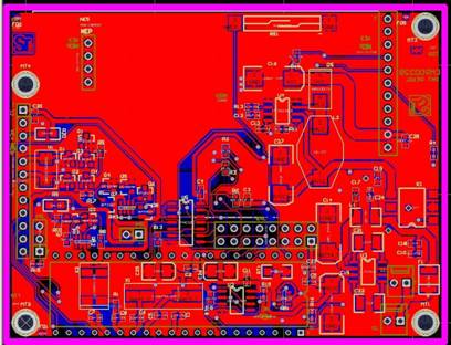
On
the left is a 40 slot PCI 64/66 backplane. I designed this for a
company that was using various I/O cards for multimedia applications. Here's PDF of the board layout where you can zoom in and out, it's about 15Mbytes: 40 slot PCB 64 backplane
This is the EDWG used for registration of the PCI connectors and mounting holes EDWG of 40 slot PCI backplane |
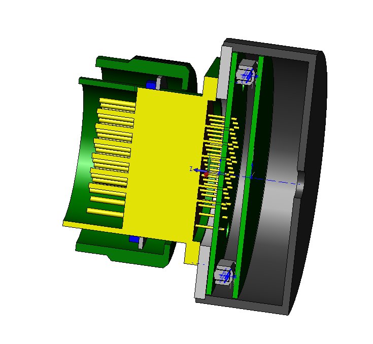
| On the right
is a partial view of an OC48 packet processing PCB. This design was
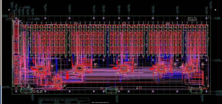
completed in less than 3 weeks. It contained a 901 pin socketed BGA (custom development socket) 18 split planes for various power rails, 5 data busses running at 200 Mhz clock speeds (one was 128 bit wide) and various other I/O used for development of firmware /software. It fed a LVPECL transponder via an Intel 6048 framer. This was a 19 page schematic and as mentioned, 10 layers with significant LVPECL nets with numerous layout constraints for impedance of dozens of differential pairs, 5 clock domains all running at 150MHz or more, and 18 split planes, each filtered and regulated. I turned that job in less than 10 days. I have lots of these samples, if you’d like more. One of the techniques I use that made it possible to deliver that in such as short period of time is my method of using staging tables to generate schematic symbols DIRECTLY from the manufacturers PDF datasheets. No chance of mis-keying pin names and numbers. If the datasheet is right, so is my schematic. |
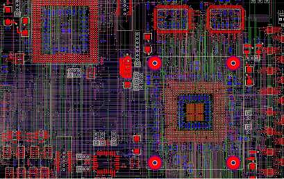 |
| This is especially handy when doing parts like the 600 pin Intel IXF6048 framer, shown on the PDF example. |
Here's a link to an Acrobat file of the composite plot of the above PCB: http://www.ajawamnet.com/ajawam1/g010707d.pdf |
Mechanical Design |
| Also have over 20 years of experience in 3D modeling and all forms of CAD design. I have and own over 20 various, licensed programs such as Solidworks, AutoCAD Mechanical, and various software tools used with my mid-sized 4-axis CNC machine. |
 |
I typically deliver
EDWG’s to clients for verification of design intent and to insure that
the overall product meets their criteria. Simply put an EDWG is a zip
file that contains an executable viewer with the 3D model data that
does NOT require any installation or other software to be present on
the clients machine. You simple extract the EDWG file, execute the
extracted file and enjoy. You can then rotate the model, zoom in/out,
or hide/make transparent any part of the model. |
|
An EDWG sample of
the above chassis design can be found at: | |
| Below is an interesting example of some of the 200 turnkey designs I've done. Typically when asked to do a full design for a product, I drive it from the desired mechanical form down to the component level. A photo of the completed design is shown here. | |
 |
Another
EDWG sample can be found at:
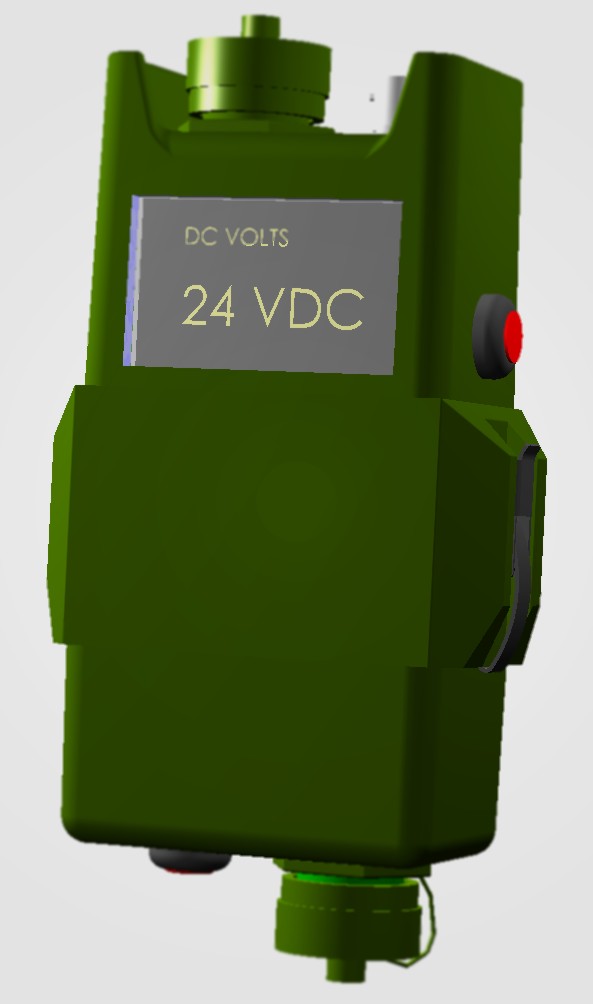
A
photo of the completed design is shown here Again, this was a "rush job" for a local D.C.-based firm that needed a hardened enclosure for use on military HumVee's. It required a water-tight enclosure for use with wireless equipment and had to have provisions for shore power as well as 24VDC with internal gel-cel battery backup. I also designed the majority of the internal electronics. The entire design (mechanical and electrical) as well as supplying OER, INC in |
 |
This is where my
acumen with both the practical considerations of the product as a whole
determines the success of my projects
and I have to say (and can provide references) that
one comment I always get is: In fact, a lot of the mechanical vendors I've used in the past, comment on how error-free the entire packaging is. A prime example of an innovative injection mold design; where again, everything fit on the first run of parts is located at: Link for ev0034.zip Having it all fit and work the first time as well as meet all the design requirements was critical to the accelerated delivery schedule proposed by the customers. I was able to accomplish this with time to spare. |
 |
This is due to my
18+ years of experience, taming many CAD disciplines and software
suites into a seamless tool-chain that provides directly driven PC
board mechanicals/footprints from various mechanical CAD tools. |
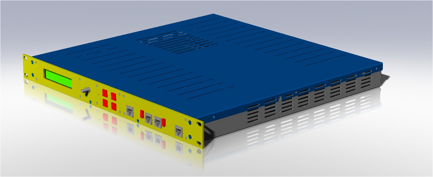 |
| Here's another
example of a rush job. A single rack unit chassis for use in network
management. I designed the hardware as well as all mechanical parts in
less that 3 weeks. I designed 4 custom PCB assemblies that
allowed the device to failover to a pass-thru state if the custom
supervisory processor detected any failure within the main subsystem. A link to the edwg can be found here - Link to 1U chassis design |
Facility Design and Engineering |
|
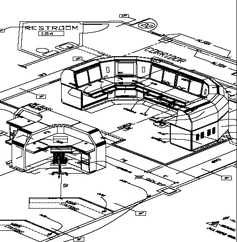
| In addition to
product design, I occasionally get asked to also design the facility
the customer is going to operate from. This ranges from
Broadcast/Production to secure NOC/NSOC's. This includes shop, field
and permit drawings as well as scope of work for MEP fit outs with
regard to specialized applications and facility functions. At the right
is an illustration from a pdf file showing a typical fit out: NSOC.PDF It contains a short version of a typical drawing package for furniture and facility mods as well as notes for contractors. In fact, I designed additional consoles for this room, at a fraction of the cost of typical NOC furniture. An EDWG that the contractor used in his furniture/fixture shop can be found here: NSOC counter As shown in the EDWG, this was designed for modular fabrication and easy on-site installation. Another PDF sample, shown below, can be found here: NOC Scope of work PDF 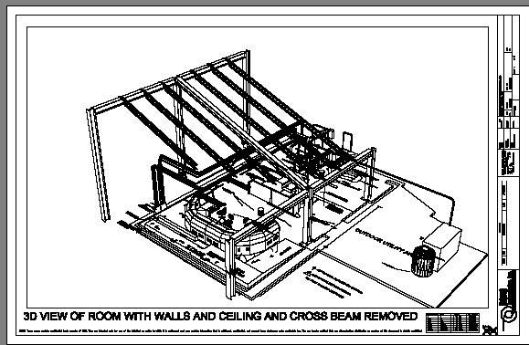 |
|
CNC Machining and Prototypes |
Link to Swarf page |
|
So, in essence, I built my own lab, soup to nuts, everything I'd need to do this. Not only can I do the package (or a lot of times use modified COTS enclosures) and electronic design, but I can get it fabbed inexpensively, hand build the first few (even 700 SMT parts is no problem), load code, test it and deliver an actual working product. In summary, I believe my hands-on approach lends itself to something that can actually be produced and marketed. As to my CNC shop, the following are some links to video samples of my machine: Milling a front panel faceplate for a communication device: Video - Front Plate Video - Specially jigged front plate Milling a 2x3 6061 AL block: Video - 6061-1 Video - 6061-2 Milling a COT’s enclosure for use in an avionics prototype (electronics designed in-house): Video - DSCN0860.avi Cutting a pocket for use in a thermal solution for Hi Powered RF design (electronics designed in-house and by others): Video - pocket.avi Milling a 2" block for use in a mechanical subsystem: Video - 2inblks.avi Milling a pattern of endplates for a COTs enclosure (Hammond) |
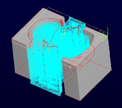 Typical tool
path generation from solid model
|
| Traditional Resume and Portfolio Resume in Acrobat format: http://www.ajawamnet.com/wamres2.pdf |
| A list of licensed software currently used in-house for the past 10 years: ORCAD Altium Designer Mathsoft MulitSim Quartus Tina Codevision for Atmel DeskPCB B2SPICE Waveformer Pro Solidworks AutoCAD Mechanical Visual Mill Professional Metacut |
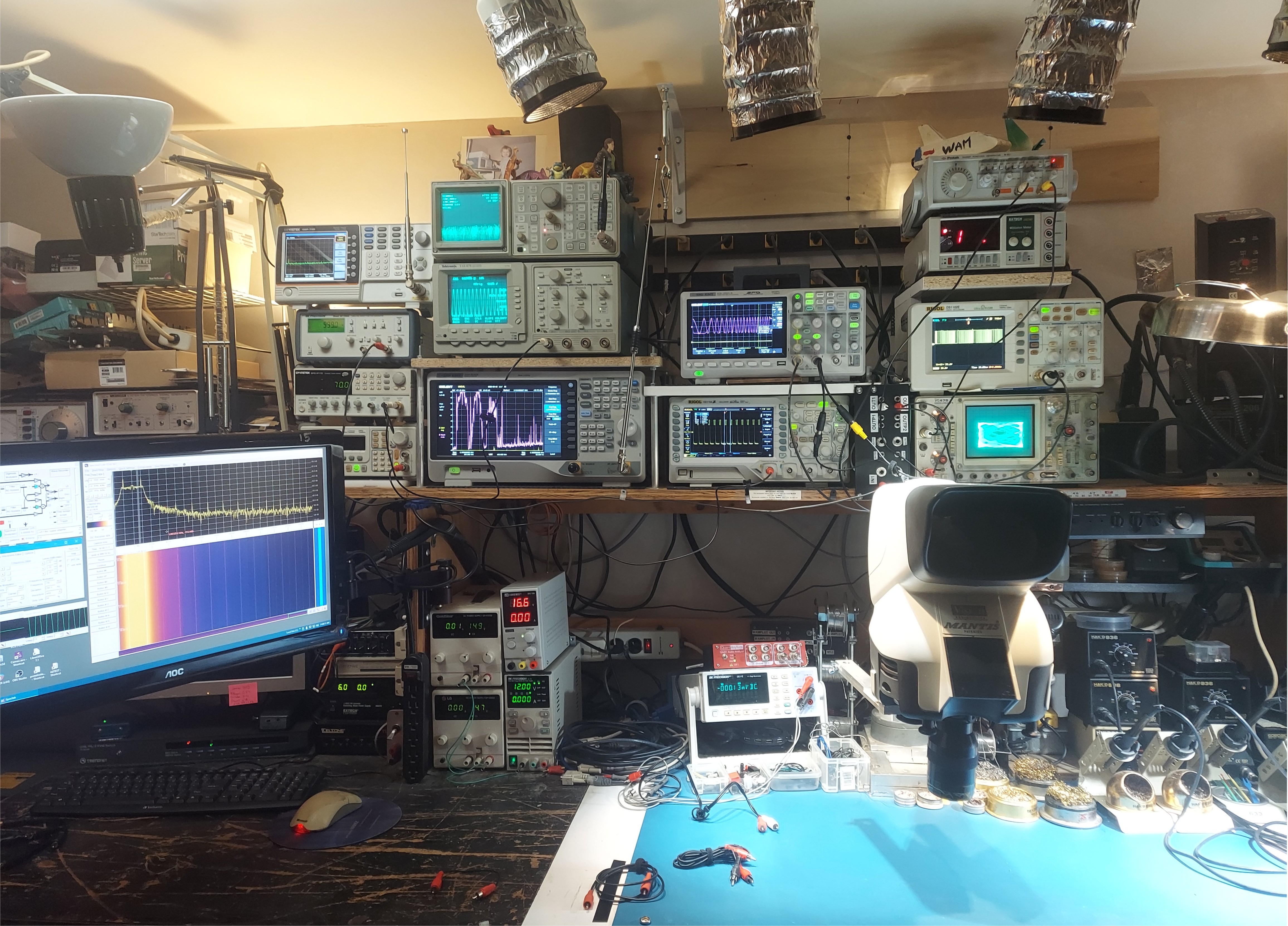
Equipment in house: Various Tektronix’s Oscilloscpes Tektronix Spectrum Analyser Various PC-based Logic Analysers Mantis Stereo Inspection Viewers Hakko Thruhole/SMT rework Various BGA rework centers from APE with fully-programmable ramp-soak-reflow Arch E size (42”) color plotter Specially modified CNC – 22x10x10 (X-Y-Z) work envelope with 4th axis |
| Misc links |
| Jon Fritz - When
It's Over Reviews Marketturd - Rants for Prehensile Chimps |